PCB Board AOI Machine–Automated Optical Inspection System for SMT Defect Detection – Supplier
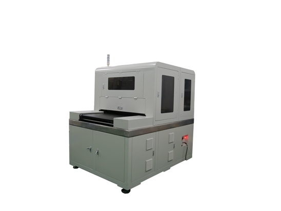
PCB board AOI machine
(Ref : AOI-PCB-R)
This AOI machine (AOI-PCB-R) is an automated optical inspection machine specially designed for PCB boards . It can be used to inspect various defects on circuits at PCB bare board, such as short/broken circuit, line width/line distance difference, bump/sink, pinhole, copper residue, scratches, hole plugs, holes, size and position errors, etc. With high-resolution line scan cameras and a highlighted multi-angle LED light source, a variety of lighting methods to achieve optimal image contrast. With AI intelligent automatic filtering of false points function, completely replace the traditional manual detection, reduce manual re-judgment and improve efficiency.
Features
1. AOI, close to the human eye vision mechanism, is more than 4 times the capacity of the traditional offline AOI, resulting in significant savings in labor costs.
2. Flexible combinations such as automatic loading and unloading offline AOI and wire etching line online AOI ;
3. Online production, offline to establish a new material number, change the number without downtime;
4. According to customer demand to customize the online real-time measurement line wide distance, to ensure product quality;
5. Front and back side online detection;
6. Real-time preservation/display of surface defect images and location;
7. The system automatically analyzes defects/defects data, and reports are generated to provide reference;
8. To guide the process to improve the process and improve the yield;
9. Better detection performance with Feflon and high frequency materials ;
Specification
Camera | High precision line-scan TDI camera (high resolution line scan lens |
Light source | High brightness and multi-wavelength LED line light source |
Minimum width/ line space | 2.5/2.5mil |
Producing condition | ODB++ and Gerber format |
Panel | dimension : 10"×10"-29"×30", thickness : 0.075mm-5.0mm, Inner and outer layers both available |
Detecting type | Signal Layer,Ground Layer and Mixed Layer |
Overall size | 1940mm(L)×1430mm(W)×1900mm(H) |
Weight | 1400kg |
Max power consumption | 6.5KW |
Power supply | 220VAC 50/60Hz |
Environment temperature | 22℃±2℃ |
Environment humidity | 45%-65% |
Reposted for informational purposes only. Views are not ours. Stay tuned for more.